Head of the laboratory:
Scientific team:
- Karasev Platon Alexandrovich
- Podsvirov Oleg Alekseevich
- Sokolova Daria Arnoldovna
- Fedorenko Elizaveta Dmitrievna
- Studzinsky Vitaly Mikhailovich
- Shestakov Sergey Andreevich
- Research directions
- Modification of surface properties of materials by beams of accelerated atomic and cluster ions in the energy range 15 – 350 keV;
- Research of processes during irradiation of semiconductors and thin films with molecular and heavy ions;
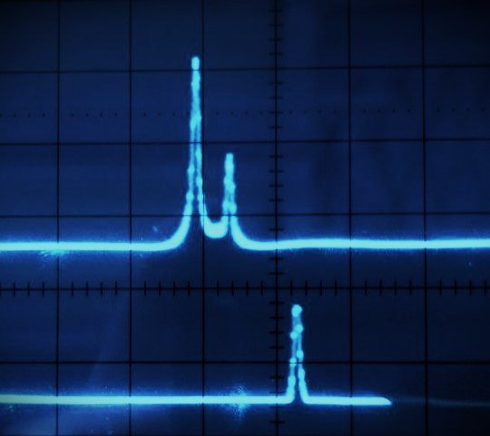
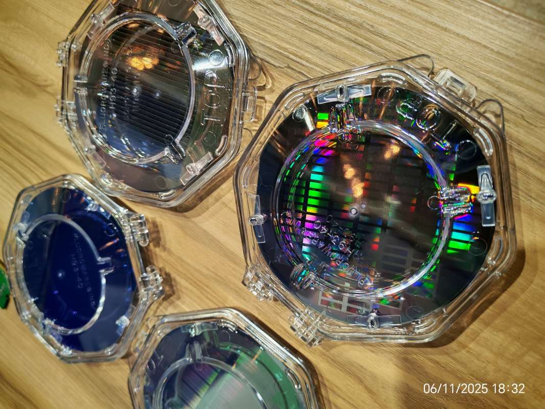
- Analysis by Rutherford backscattering spectrometry of fast helium ions (RBS & RBS/C analysis): depth distributions of heavy impurity atom concentration in matter, depth distributions of structural damage in single crystals, composition and thickness of thin films on the surface;
- Modification of materials by electron beams with energies of 10 – 50 keV;
- Study of the role of electron irradiation in the creation of nanoclusters and nanoparticles in glasses and optical crystals containing ions of various metals;
- Investigations of the influence of creation conditions and subsequent thermal and ion treatments on the properties of thin carbon films;
- Analysis of surface topography using atomic force scanning microscopy.
- Equipment used
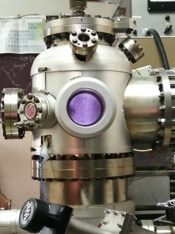
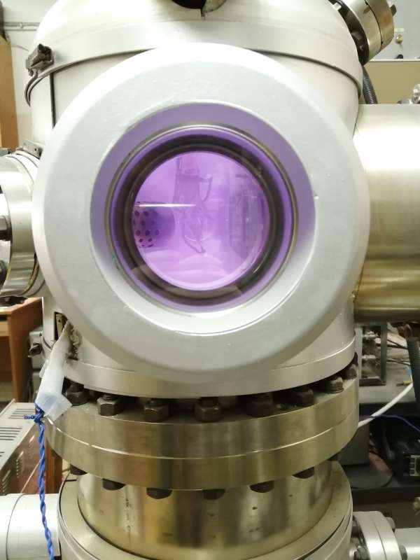
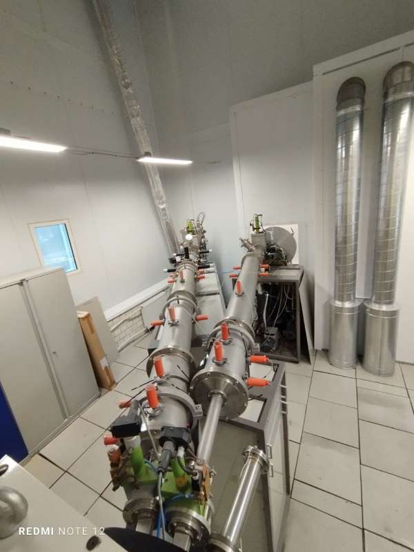
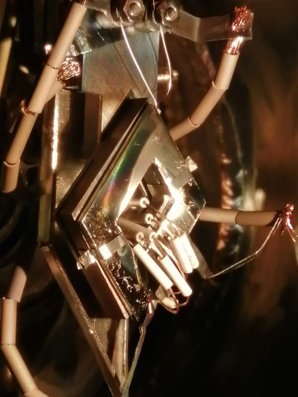
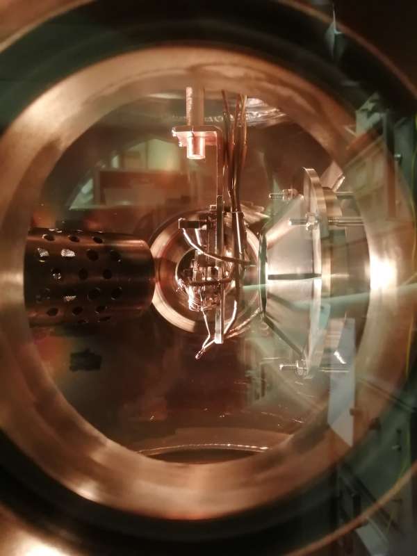
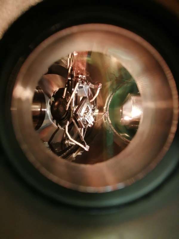
- Ion implanter, HVEE-500 heavy ion accelerator energy 10-400 keV, ions 1-250 amu, doses 1011-1016 cm-2
- Electron accelerator, JEBD-2 high-current scanning electron microscope, energy up to 50 keV
- Rutherford backscattering spectrometry (RBS), including in combination with channeling (RBS/C), HVVE-500 heavy ion accelerator, He++ 0.5-0.8 MeV
- X-ray diffraction analysis (XRD), Bruker D8 Advance diffractometer with Bragg–Brentano focusing
- Scanning electron microscopy (SEM), TESCAN MIRA3 microscope with energy-dispersive X-ray spectroscopy (EDX) attachment
- X-ray photoelectron spectroscopy (XPS), NT-MDT Nanofab-25 installation with SPECS FG20 electron gun
- Atomic force microscopy (AFM), Pacific Nanotechnology Nano-DST microscope with TipsNano NSG01 probes
- Profilometry, Surfcom touch 50 profilometer
- FTIR spectroscopy, Shimadzu IRSpirit-X Series and Bruker VERTEX 80/80v spectrometers
- Raman spectroscopy, Renishaw InVia Raman spectrometer
- UV and visible spectrometry (UV-visible), SF-56 UV-VIS spectrophotometer 190-1100 nm
- Scanning laser particle analyzer, "Nanoreflex CLSM"
- Transparent thin film thickness control setup, ES-2LED ellipsometer
- Four-point probe measurement setup, ST2258C with tungsten carbide probes
- SNOL equipment for thermal annealing up to 1200°C
- "Alpha N1" magnetron sputtering system for thin films with quartz thickness control
- Oxford Instruments thermal evaporation systems for thin films
- Hall effect and transport properties measurement setup
- Ultrasonic baths for sample cleaning
- Access to lithography, wet and dry etching technologies
- Use of software packages: SRIM, SIIMPL, RUMP, Lammps, COMSOL Multiphysics, Python, MATLAB
- Modeling using Monte Carlo methods, molecular dynamics (MD) and density functional theory (DFT), including using the capabilities of the SPbPU Supercomputer Center "Polytechnic" (peak performance 2.2 TFlops)
- Publications
- Achievements
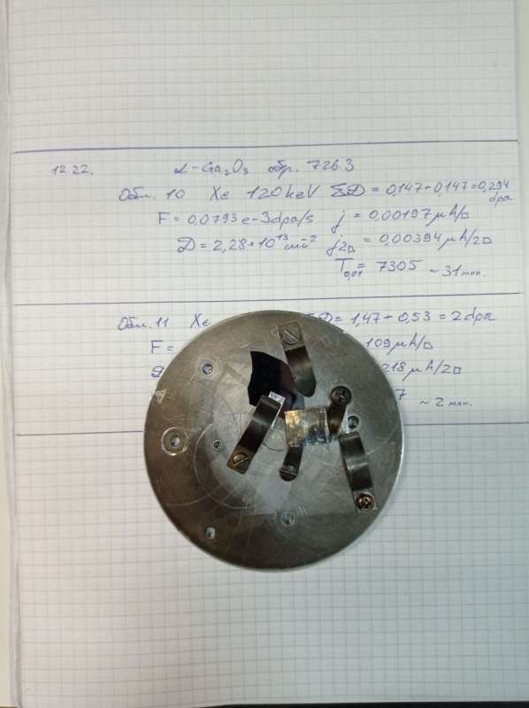
For the first time in the world, a systematic study of radiation defect accumulation in GaN under sequential irradiation with ions of different types and ions of different energies was carried out. It was shown that defect formation in the crystal volume is determined by the competing interaction between radiation-stimulated annealing and stabilization of defects by implanted atoms. Moreover, the balance between these two processes depends on the type of implanted atom. In particular, for samples pre-implanted with fluorine ions, a strong enhancement of damage was observed, leading to complete volumetric amorphization of GaN, whereas co-irradiation of samples pre-implanted with ions of elements such as neon, phosphorus and argon led to a decrease in damage.
A comparative study of the radiation resistance of gallium nitride and alpha and beta gallium oxides was carried out. It was shown that GaN has the highest radiation resistance, the alpha polytype is slightly inferior, and the defect accumulation rate in beta Ga2O3 is much higher than in the others. The earlier result on the saturation of the damage level in β-Ga2O3 at 90% of complete amorphization was also confirmed. It was shown that the rate of damage accumulation in this material can be controlled by internal mechanical stresses.
For the first time in the world, a correlation was established between the damage level of alpha and beta Ga2O3 during ion beam processing, the fractal dimension and the density of individual displacement cascades formed by ions. The decisive role of the density of collision cascades in the accumulation of structural damage in these materials was demonstrated. The results of these calculations make it possible to predict the growth rates of the damaged layer near the surface and the accumulation of disorder in the volume of these materials based on modeling in the approximation.
A completely unusual intermediate defect peak in alpha-gallium oxide was discovered for the first time. The conditions for the occurrence of this peak were analyzed, which differ significantly from those for another wide-bandgap semiconductor – zinc oxide, in which an intermediate peak was also previously observed.
In addition to studying radiation processes in wide-bandgap semiconductors, a cycle of experimental studies was carried out on the formation of coatings by irradiation with C60 fullerene ions with energies of several keV. The possibility of forming different types of coatings and controlling their properties by varying the ion energy and substrate temperature was demonstrated. To explain the observed phenomena, the interaction of C60 ions with the target surface was modeled using molecular dynamics. A set of appropriate methods for calculating single impacts and cumulative dose accumulation was developed. A new effect was experimentally discovered and explained based on the obtained model data – the formation of a deep groove along the interface between the irradiated and original regions during irradiation through a solid shadow mask.
Methods for the synthesis of noble nanoparticles both on the surface of substrates, including heat-sensitive substrates, including polymer materials, as well as in the near-surface region of dielectric substrates using ion bombardment and electron beam treatment, have been developed.
- Collaborations
- JSC "NPP "ELAR";
- JSC "CRI "ELECTRON";
- Ioffe Physical-Technical Institute of the Russian Academy of Sciences;
- Faculty of Physics, Lomonosov Moscow State University;
- St. Petersburg Academic University named after Zh.I. Alferov;
- Nazarbayev University, Astana, Kazakhstan;
- University of Petroleum and Energy, Dehradun, Uttarakhand, India;
- Amity University, Uttar Pradesh, India;
- University of Oslo, Oslo, Norway;
- Lawrence Livermore National Laboratory, Livermore, USA;
- Ashish Kumar, Inter-University Accelerator Centre, New Delhi, India;
- University of Hyderabad, Hyderabad, India.
.jpg)